Strain and composition effects on Raman vibrational modes of hexagonal GaP-Si-Si(1-x)Ge(x) core shell nanowires
Z.Azdad Möri
The author independently carried out all calculations, measurements, and data interpretations presented in this work
Source : Håkon Ikaros T.Hauge, Sonia Conesa-Boj et al. NanoLett.17(1),85(2017)
As part of my research, I investigated the vibrational spectra of hexagonal SiGe structures grown on hexagonal GaP/Si core-shell substrates using metal-organic vapor phase epitaxy (MOVPE). Through detailed Raman spectroscopy measurements,
I explored how varying germanium composition influences vibrational frequencies—providing key insights into strain effects within the crystal lattice. These experimental results were further contextualized by comparing them with theoretical Raman spectra , calculated using ab initio methods (using quantum-espresso package). To bridge the gap between complex data and practical understanding, I developed a simplified yet robust model that accurately identifies the vibrational signatures of distinct Raman modes.
My findings have been shown in various conferences and recognized by experts the domaine.
Motivation:
In the ongoing quest to revolutionize telecommunications and data transmission technologies, the discovery and development of new materials with superior optoelectronic properties are critical. Among these, hexagonal silicon-germanium (SiGe) alloys have emerged as a highly promising candidate. Unlike their conventional cubic counterparts, hexagonal SiGe alloys are theoretically predicted to possess a direct bandgap, particularly for compositions with a high germanium content. This is a transformative property, as a direct bandgap allows for efficient light emission—a feature that conventional silicon lacks. Such a breakthrough could enable the seamless integration of optical components directly onto silicon-based platforms, bridging the long-standing gap between electronics and photonics. This would pave the way for ultra-fast, energy-efficient optical communication systems, dramatically reducing latency and power consumption in data centers and telecommunications networks.
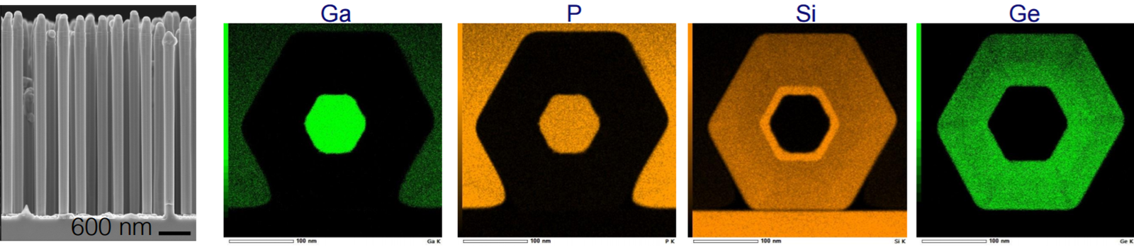
Furthermore, μ-Raman spectroscopy plays a pivotal role in characterizing these nanostructured materials. It offers spatially resolved insights into the crystalline quality, local strain fields, and alloy composition of intricate nanostructures, such as single GaP-Si-Si₁₋ₓGeₓ core-shell nanowires. These nanowires, with their engineered strain and composition gradients, hold the key to tailoring band structures and enhancing optoelectronic performance. By understanding and controlling these parameters at the nanoscale, researchers move closer to realizing monolithically integrated optoelectronic devices that are not only compatible with existing CMOS technology but also capable of supporting the exponential growth in global data traffic. The development of hexagonal SiGe thus represents a crucial step toward the next generation of photonic-integrated circuits, bringing us closer to the dream of an all-optical internet and quantum-level communication speeds.
Investigation of growth homogeneity
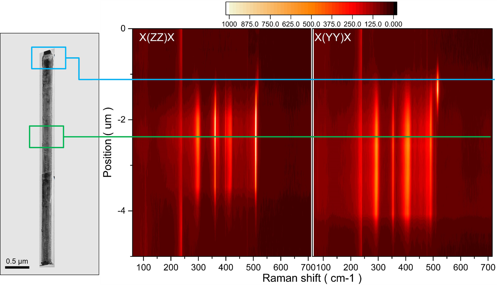
High quality map of the vibrational frequency has been collected along the wire under two polarizarion configuration X(ZZ)X and X(YY)X. This Spatially resolved μ-Raman measurements revealed the presence of a defective region extending up to approximately 0.5 μm from the gold catalyst droplet at the tip of the nanowire. This defected zone is characterized by a mixed crystalline domain, where both hexagonal and cubic silicon (Si) phonon modes are detected simultaneously due to violation of the selective polarization rule. With the absence of the GaP core signal. The coexistence of these two phases indicates a transition region likely caused by strain relaxation or lattice mismatch near the growth interface.
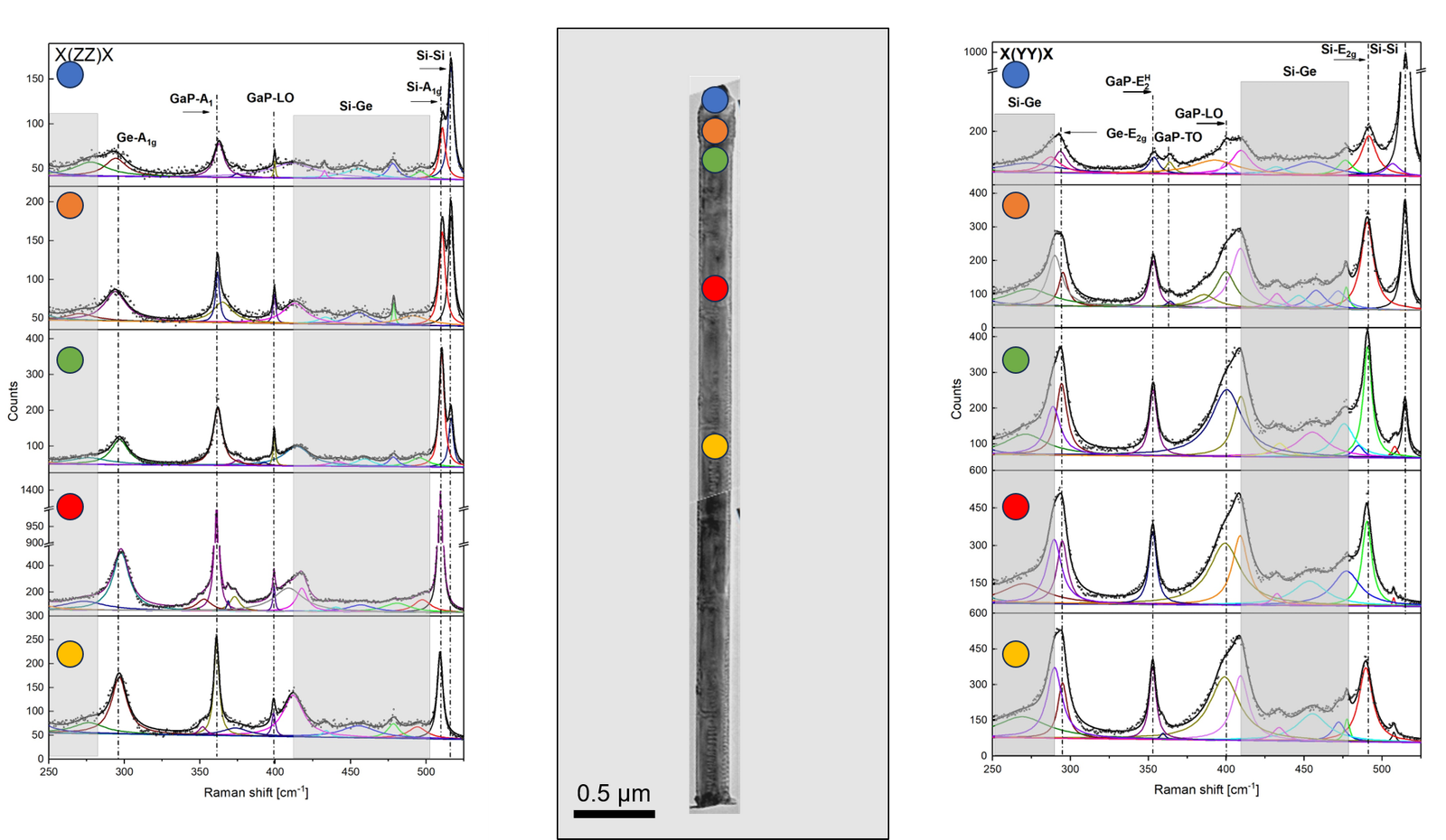
From the measured spectra, one can clearly see that multiple modes exist, highlighted by the shaded area in the figure. These modes extend from 400 cm⁻¹ up to 480 cm⁻¹, as well as a lower band below 300 cm⁻¹. Similar observations have been made when studying Cubic SiGe alloy. The modes between 400 cm⁻¹ and 490 cm⁻¹ are characteristic of vibrations of silicon atoms in a germanium-rich environment, while the lower-frequency band corresponds to germanium vibrations in a silicon-rich environment.
In order to accurately describe the vibrations of each observed mode, it is necessary to perform a large
supercell
simulation with randomly placed Ge and Si atoms. However, this approach is computationally very expensive.
A more simplified approach is proposed. It is known that the overall Raman signal is a convolution of all
the individual
vibrations within the crystal. At the local scale, one can assume the existence of perfectly structured
single-unit
cells of SiGe. Given the typical laser spot size used in Raman spectroscopy (ranging from 300 to 900 nm), it
can be
assumed that the collected Raman signal statistically includes contributions from all possible local
configurations of a
perfect SiGe crystal. Therefore, the intensity and full width at half maximum (FWHM) of the signal can
provide
information about the number of such cells present in the probed volume and their local environments.
Raman Spectra from the first-principal
To simulate Raman spectra from first principles, the Quantum ESPRESSO package was employed. The specific
computational
details of the simulations are omitted here for brevity. However, interested readers are welcome to contact
me for a
detailed description of the methodology used.
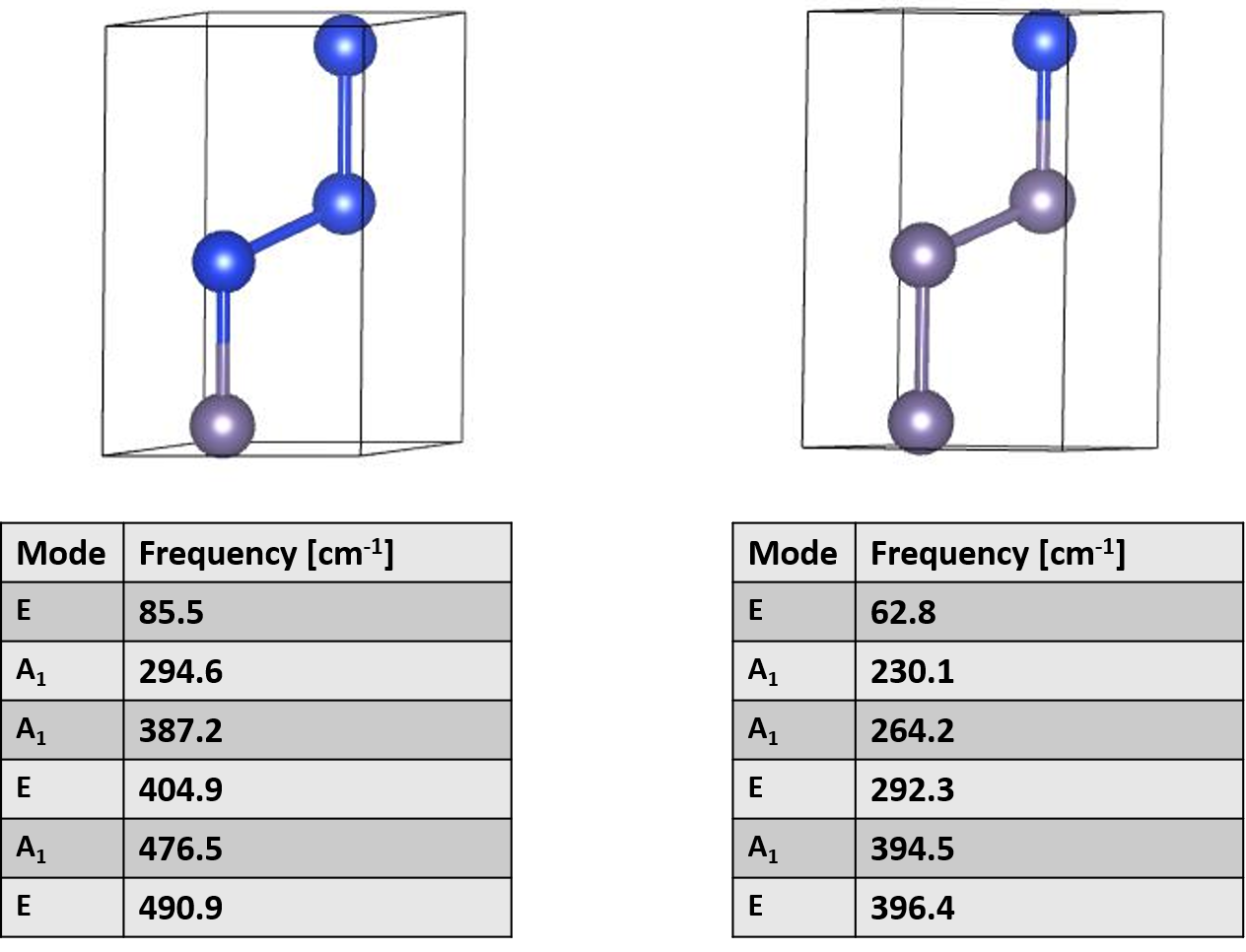
As an initial step, hexagonal phases of both silicon and germanium were simulated to validate the choice of
pseudopotentials and the energy cut-off parameters. Structural relaxation was first performed to obtain
optimized unit
cells. Following this, phonon calculations were conducted to analyze the vibrational properties, which are
essential for
Raman spectrum prediction.
The obtained unpolarized Raman spectra of pristine hexagonal Silicon and Hexagonal are displayed below:
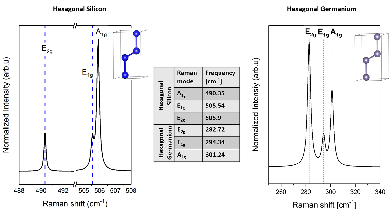
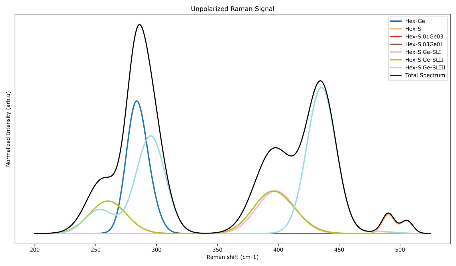
The simulated spectra show excellent agreement with the measured data. However, since pristine hexagonal germanium has not been experimentally measured, the simulated spectra of hexagonal germanium will serve as a reference for understanding the Si–Ge vibrational and electronic bands. To address this challenge, three types of unit cells are proposed:
- Type-I: Characterized by alternating stacking of silicon and germanium atoms, where each Si atom is surrounded by Ge atoms in all directions, and vice versa. Therefore a C 3V(6mm) point group
- Type-II: A Si–Ge structure constructed with D 3h (-62m) point group.
- Type-III: A Si–Ge structure based on the D 3d (-3m) point group.
These configurations together with there Raman spectra and vibrational modes are illustrated in the image below:
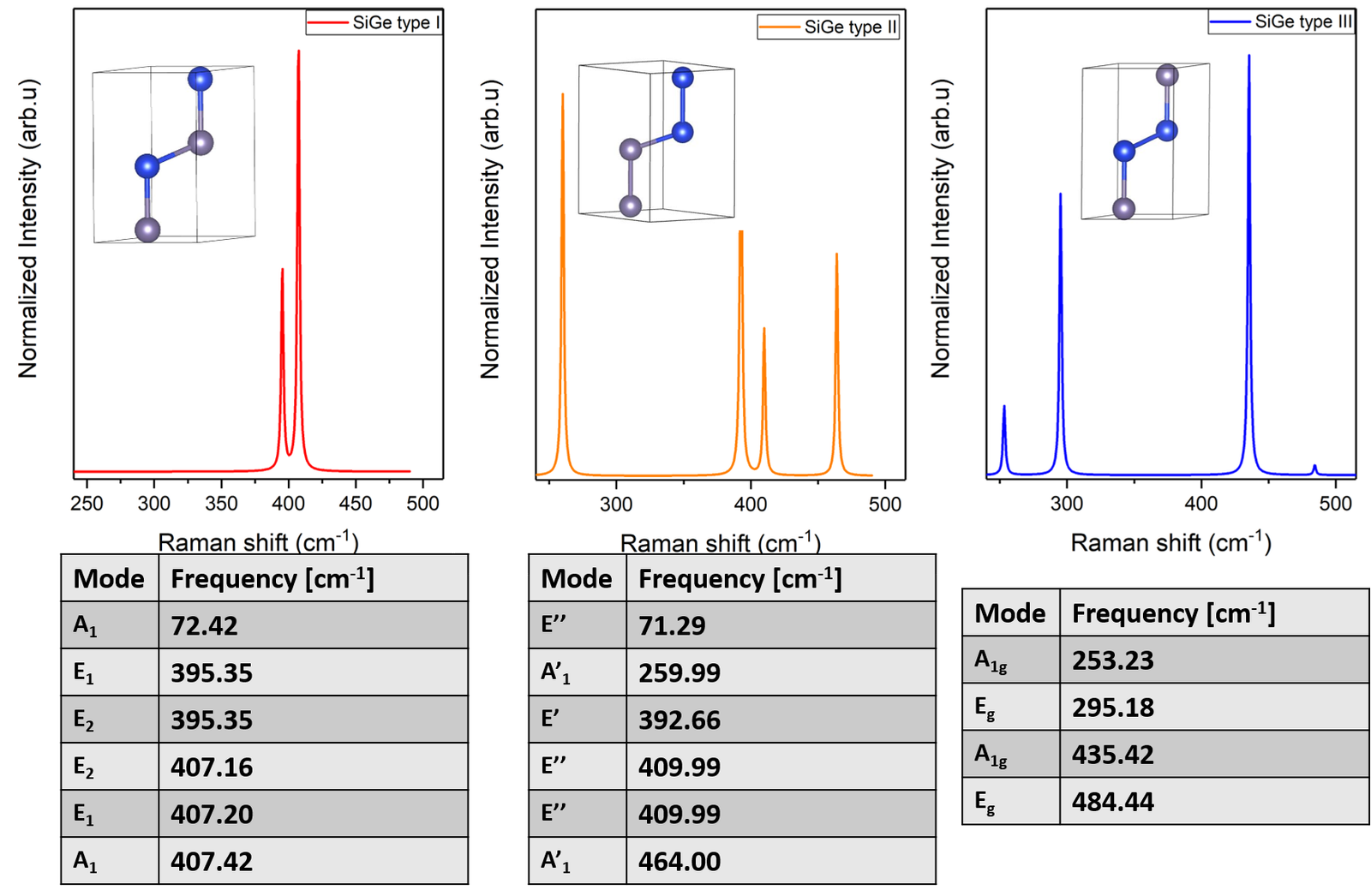
The Raman spectra for such a calculation was not performed. However, the phonon calculation and mode symmetry reveals the frequencies and the mode of such configurations.