Surface Phonons in III-V Semiconductors computational approach
Z.Azdad Möri
The author
independently carried
out all calculations, measurements, and data interpretations presented in this work
Surface phonons arise due to the disruption of translational symmetry at the surface of a solid, leading to
vibrational
modes that are confined near the surface. These excitations exhibit extraordinary properties that
distinguish
them from
bulk phonons. Of particular interest is their strong coupling with electromagnetic waves, which has enabled
a
range of
advanced applications in nanotechnology and thermal management. For example, surface phonon polaritons can
be
harnessed
as sources of coherent and monochromatic thermal radiation. Furthermore, their ability to mediate near-field
radiative
heat transfer enhances thermal energy exchange at the nanoscale, making them promising candidates for
improving
the
performance of thermophotonic devices, nanoscale heat engines, and thermal imaging systems.
Although the existence of surface phonons has been extensively studied using neutron scattering techniques,
measuring
their characteristics at the nanoscale remains a challenging task. Techniques such as Electron Energy Loss
Spectroscopy
(EELS) have been employed to study them; however, the spectral resolution of such techniques is often
insufficient to
provide deep insights. In contrast, Raman spectroscopy is considered one of the most effective tools for
probing
surface
modes, particularly at the Γ-point.
This study investigates surface phonon polaritons (SPhPs) in gallium phosphide (GaP) nanowires, focusing on
their
emergence, characterization, and dependence on environmental and experimental conditions. Using a
combination of
first-principles density functional theory (DFT), Boundary Element Method (BEM) simulations, and
polarization-resolved
Raman spectroscopy, the work provides a multi-faceted approach to identifying and analyzing SPhP modes.
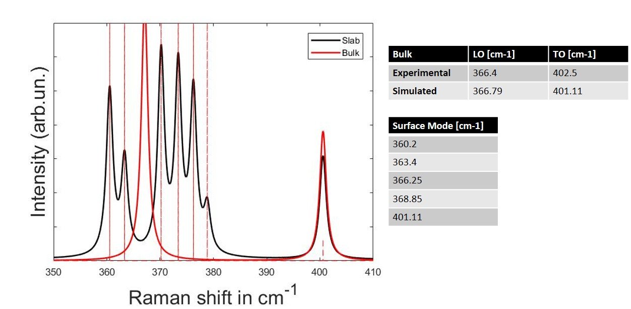
Simulations of zinc-blende GaP slabs revealed Raman-active surface modes within the Reststrahlen band, known
to strongly
interact with electromagnetic radiation. Since DFT simulations of realistic wurtzite nanowires are
computationally
demanding, Raman spectra were used to extract dielectric functions for BEM modeling.
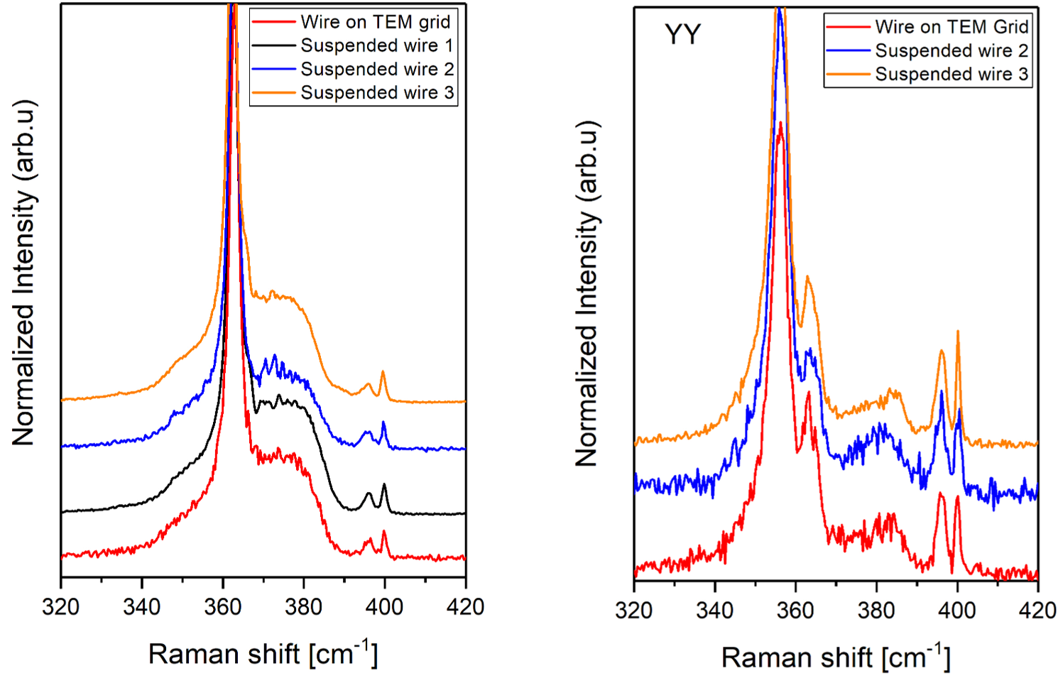
Experimentally, Raman spectroscopy was performed on GaP nanowires placed in various configurations: on
substrates,
suspended on TEM grids, and cantilevered above silicon. Clear surface phonon signatures were observed only
in suspended
geometries, where dielectric symmetry was preserved, confirming the environmental sensitivity of SPhPs. A
significant
angular dependence of these modes was demonstrated, with polariton and Fröhlich-Klemens (F-K) modes merging
at higher
incident angles, notably at 45°, signaling strong resonance effects.
Further, by placing nanowires over periodic gold strips, the study demonstrated spatial modulation of the
SPhP
intensity—absent on gold and pronounced in suspended regions. This was corroborated by BEM simulations,
aligning with
observed periodic spectral changes along the nanowire.
DFT Calculation
of Zinc Blend
Surfac phonons along the 111 Direction
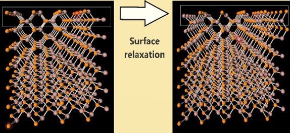
Building a crystal structure for simulating a slab is often done by constructing a unit cell that is periodic
along two
directions (X and Y) and introducing a sufficient vacuum gap along the Z direction to prevent interactions
between
periodic images of the slab.
Although this approach becomes computationally challenging as the unit cell size increases, it remains the most
reliable
method for addressing surface-related phenomena. This technique is widely used to study the surface electronic
structure
of materials and chemical reactions occurring at material surfaces. Simulations of full phonon dispersion have
been
extensively performed for various classes of materials, with results often compared to experimental data from
neutron
scattering techniques.
However, to the best of my knowledge, Raman spectra of a surface phonon slab of GaP have not yet been reported.
Relaxed structure of Slab model of Zinc-Blend GAP
In this Section, a simulation of phonon Zinc Blend Slab made out of 5 layers is performed using a slight twist
to simplify the calculation.
In essence, a standard cell optimization is performed by introducing a sufficiently large vacuum gap along the
non-periodic direction. After full relaxation of the atomic positions, the outermost layers—at the top and
bottom
surfaces of the slab—are allowed to move freely, while the core atoms are kept fixed during the phonon
calculations.
This approach effectively omits the Raman-active bulk modes and enables the study of surface phonon modes
exclusively.
Simulated Raman Spectra from a GaP slab
The simulated spectra show several varying surface modes. Although the symmetry of these modes is not explicitly
detailed, their patterns have been identified. The modes located between the longitudinal optical (LO) and
transverse
optical (TO) modes, formally known as the Reststrahlen band, are of particular interest to this study. This is
due to
the strong interaction with electromagnetic waves, which leads to the formation of surface phonon polariton
modes.
Reststrahlen bands can occur near any absorption resonance with notable strength, where the Kramers-Kronig
relations
demand an inflection in the real permittivity strong enough to create a narrow region of negative real
permittivity.
Simulated Raman Spectra from Slab and Bulk Zinc-Blend structure
It is anticipated that a slab of wurtzite GaP would exhibit a greater number of modes, given the effectively
doubled
number of surface atoms. However, such a simulation was not conducted due to the substantial computational
resources it
would require. Simulating a realistic hexagonal nanowire using density functional theory (DFT) remains
computationally
prohibitive. Nonetheless, the results from the aforementioned simulations provide valuable insights into the
expected
behavior. To achieve a more comprehensive understanding of the spectral features observed in the nanowires, we
will
employ the Boundary Element Method (BEM).
To perform Boundary Element Method (BEM) simulations, one must provide the refractive index (n) and the
extinction
coefficient (k) as functions of the wavenumber. While such optical spectra are available for GaP in its
zinc-blende
form, the dielectric dispersion relations for the wurtzite phase remain unknown. Therefore, it is necessary to
first
extract the n and k values specific to wurtzite GaP before carrying out BEM simulations.
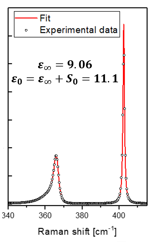
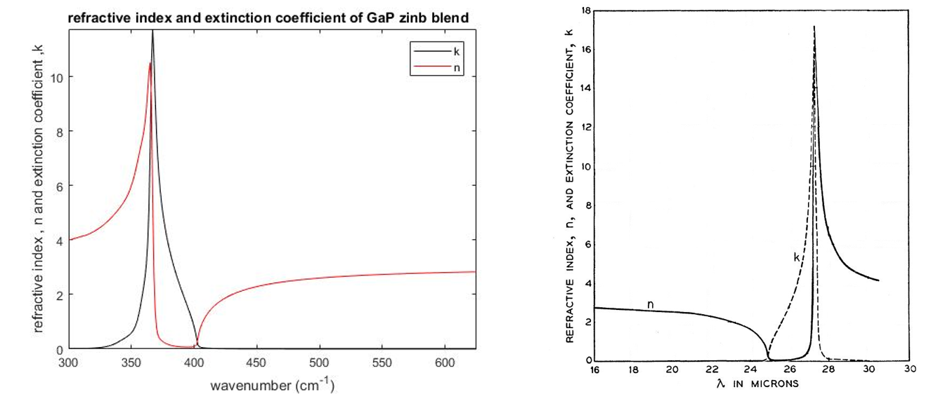
Fortunately, there exists a method to reconstruct n and k from Raman spectra. This is achieved by fitting the
Raman
response as described by
A. S.
BARKER.
$$
\varepsilon = \varepsilon_\infty + \frac{S_0\left(1 - \sum_{i=1}^{n} S_i \right)\nu_0^2}
{\nu_0^2 - \nu^2 + i\nu\gamma_0 - \sum_{i=1}^{n} \frac{S_i \nu^2 \nu_0^2}{\nu_i^2 - \nu^2 + i\nu\gamma_i}}
$$
The results of the fit are shown in the following graph:
Fitted Raman spectra using the oscillation model.
Same values were obtained by A. S.BARKER $$\varepsilon_\infty =9.09 \quad \varepsilon_0 = 11.1 $$
This value are also similar to the calculated DFT structure of bulk Zinc-blend structure. With electronic
dielectric permittivitty (F/m units) and the zone-center polar mode contributions as follow:
$$
\varepsilon_\infty =
\begin{bmatrix}
9.81 & 0.0 & 0.0 \\
0.0 & 9.81& 0.0 \\
0.0 & 0.0 & 9.81
\end{bmatrix}
$$
$$
\varepsilon_0 =
\begin{bmatrix}
11.36 & 0.0 & 0.0 \\
0.0 & 11.65 & 0.0 \\
0.0 & 0.0 & 11.65
\end{bmatrix}
$$
The anisotropy of the zone-center polar mode arises from the direction-dependent LO–TO splitting, which results
from the
directional nature of long-range Coulomb interactions. This can't be accessed experimentally as the measurement
were performed on a GaP substrate with (111) crystal orientation.
This comparison confirms furthermore the excellent agreement between the DFT calculation and the experiment.
Now that we have a robust model we can reconstruct the dispersion relation n and k using the following formula:
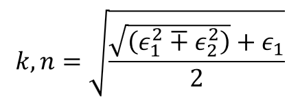
Reconstructed and literature dispersion of refractive index (n) and extinction coefficient (k)
The Same methodology was carried on a wurzite Nanowire. Because of the nature of the nanowire structure the
performed measure can only probe the crystal direction (10-10). ZZ was considered for the
spectral fitting due it's high signal intensity. The above oscillation model was used to fit the spectra. The
wire were
measured on a metallic substrate to eliminate any surface phonon polariton, giving us access to core vibrations
of
the nano-wire. The resulted dielectric dispersion is shown below:
Reconstructed dispersion of refractive index (n) and extinction coefficient (k) of Wurzite GaP Nano-wire
The reconstructed spectra reveal a similar dispersion relation for both structures. However, the wurtzite phase
exhibits
a distinctive shoulder near 350 cm
−1, characteristic of the absorption from \( E^h_2\) phonon mode.
Additionally,
the
refractive
index (n) and extinction coefficient (k) are slightly higher in wurtzite compared to the zinc-blende
counterpart. This
observation is consistent with the simulated electronic band structures, where zinc blende exhibits a higher
band
gap,
which corresponds to lower values of n and k.
Electronic band structure of Zinc-Blende and Wurzite GaP
Using the fitted dielectric dispersion above, one can identify two surface optical modes in the case of the
nanowire,
known as Fuchs–Kliewer modes, which appear in the Raman spectra. Due to the anisotropy and the lifting of
degeneracy in
the TO mode, the fitting parameters can be used to define:
$$
\omega_{s\parallel} = \omega_{T0\parallel} \left( \frac{ \epsilon_{0\parallel} + \epsilon_1 }{ \epsilon_{\infty\parallel} + \epsilon_1 } \right)^{\frac{1}{2}}
$$
$$
\omega_{s\perp} = \omega_{T0\perp} \left( \frac{ \epsilon_{0\perp} + \epsilon_1 }{ \epsilon_{\infty\perp} + \epsilon_1 } \right)^{\frac{1}{2}}
$$
Where:
\[
\begin{array}{|c|l|c|}
\hline
\textbf{Symbol} & \textbf{Description} & \textbf{Value} \\
\hline
\epsilon_1 & \text{Dielectric constant of the medium (air)} & 1 \\
\omega_{T0\perp} & \text{Transverse optical phonon frequency (\(E^h_2\) mode) of Wurtzite GaP} & 351.4\ \text{cm}^{-1} \\
\epsilon_{0\perp} & \text{Static dielectric constant (perpendicular) of Wurtzite GaP} & 18.21 \\
\epsilon_{\infty\perp} & \text{High-frequency dielectric constant (perpendicular) of Wurtzite GaP} & 14.0 \\
\omega_{T0\parallel} & \text{Transverse optical phonon frequency (\(E^h_2\) mode) of Wurtzite GaP} & 360.3\ \text{cm}^{-1} \\
\epsilon_{0\parallel} & \text{Static dielectric constant (parallel) of Wurtzite GaP} & 18.21 \\
\epsilon_{\infty\parallel} & \text{High-frequency dielectric constant (parallel) of Wurtzite GaP} & 14.0 \\
\hline
\end{array}
\]
Raman spectra of Gallium Phosphide Nanowires on Silicon Substrate measured using ZZ polarization
configuration
$$\omega_{T0\parallel} =386.4cm^{-1} \quad \omega_{TO\perp} =396.1cm{-1}$$
From the above spectra no apparent surface phonons are present and this spectra is similar
reported Raman
Measurements of GaP nanowires in the literature. Notably, the majority of these prior studies were conducted
with
nanowires placed directly on a substrate. In such
configurations, the nanowire is embedded in an asymmetric dielectric environment—exposed to air on one side and
in
direct contact with the substrate on the other. This asymmetry disrupts the conditions required for the
excitation of
surface phonon modes, which typically require a uniform surrounding dielectric to sustain strong surface
resonances.
Consequently, this explains why many earlier experimental efforts failed to detect or resolve surface phonon
polariton
signatures.
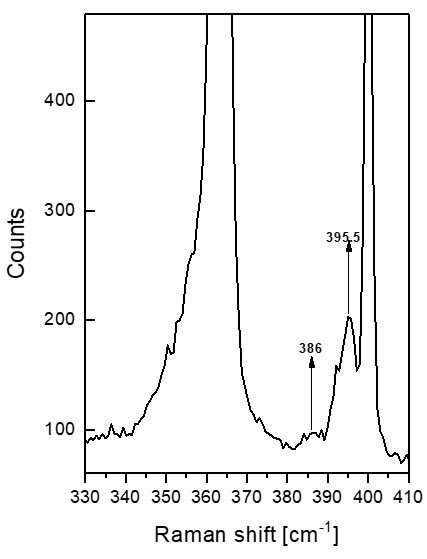
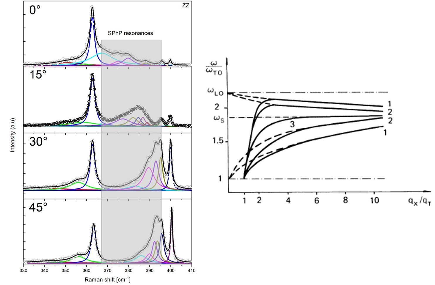
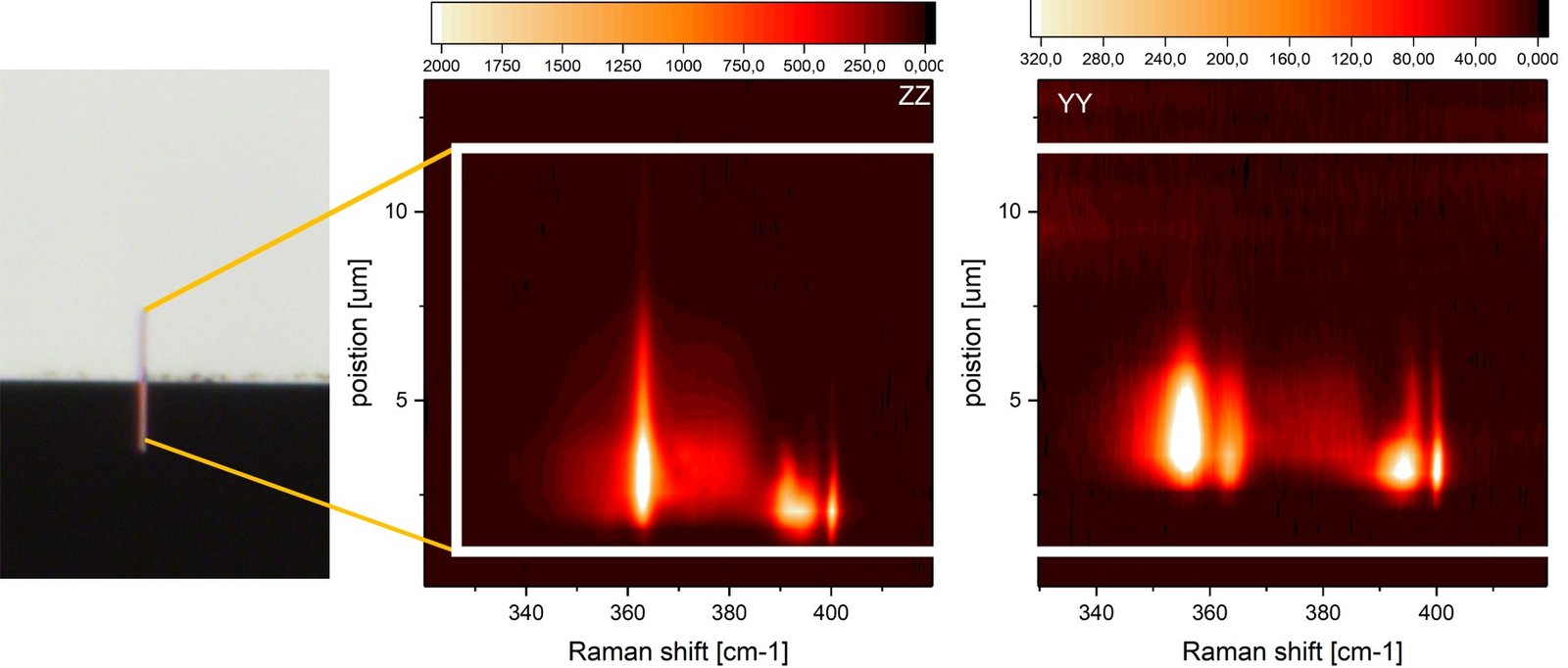
In the following section, we present a significant breakthrough in the identification and analysis of surface
phonon
modes in wurtzite GaP nanowires. The distinct signatures of individual surface modes are revealed, and their
corresponding frequencies are calculated using boundary element method (BEM) simulations. To unambiguously
demonstrate
the existence of these modes, Raman spectra were acquired from a single nanowire transferred onto a TEM grid,
ensuring a
suspended configuration ideal for supporting surface phonon polaritons. The same nanowire was subsequently
imaged via
transmission electron microscopy to confirm its wurtzite crystal structure, thereby eliminating variability
arising from
structural differences among grown nanowires. The recorded Raman spectra, obtained under the three principal
polarization configurations, are presented below.
Raman spectra of Gallium Phosphide Nanowires on TEM grid Substrate measured using ZZ,YY and ZY polarization
configuration
The above spectra shows something remarkable, a broad band extended from \( 363 cm^{-1}\) to \( 384 cm^{-1}\)
can
be seen. To make sure that this is not an experimental artifact. 3 other wires were placed in
a cantilevered configuration using a nanomanipulator and Raman spectra was collected at almost identical
location as displayed by the following image:
GaP Nanowire placed on the edge of a Silicon substrate
The collected spectra under ZZ and YY configuration are shown bellow:
Measurement of GaP wired in cantilevered configuration under ZZ and YY polarization
These results not only demonstrate the reproducibility of the measurements across multiple nanowires, but also
provide
compelling evidence for the presence of surface phonon polaritons. To further validate their existence, we
explored one
of their key distinguishing features—their strong dependence on the angle of incidence of the electromagnetic
wave.
Surface phonons are highly sensitive to the surrounding dielectric environment and the orientation of the
excitation
field. To probe this angular dependence, a GaP nanowire was positioned in a cantilevered configuration and
mounted on a
precision rotational stage, allowing controlled variation of the incident angle relative to the nanowire axis.
The angle
was incrementally varied from 0° to 33°, and the resulting Raman measurements are presented below.
Measurement of GaP wired in cantilevered under different polarization and incident angle
As anticipated, surface phonons become notably pronounced when they resonate with surface phonon-polaritons.
This
resonance is
evidenced by a broad spectral feature near the transverse optical (TO) phonon mode, particularly under ZZ
polarization,
where Raman selection rules preferentially enhance transverse vibrational modes.
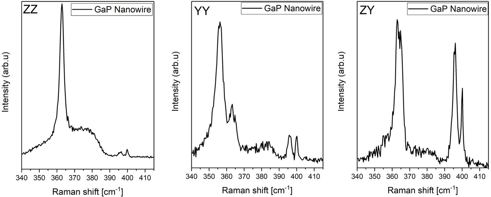
In the cross-polarized configuration—where the incident electromagnetic field is oriented perpendicular to the
nanowire growth
axis pronounced Fröhlich-Klemens (F-K) mode emerges at 396 cm⁻¹. Unlike conventional Raman-active modes, the
F-K mode
arises from a combination of non-zone-center phonons, specifically involving longitudinal optical (LO), TO, and
acoustic
phonons. Because it does not conform to standard Raman selection rules, the F-K mode is observable across all
polarization configurations.
A lower-energy F-K mode, centered at 386 cm⁻¹, is particularly well-resolved under YY and ZY polarizations.
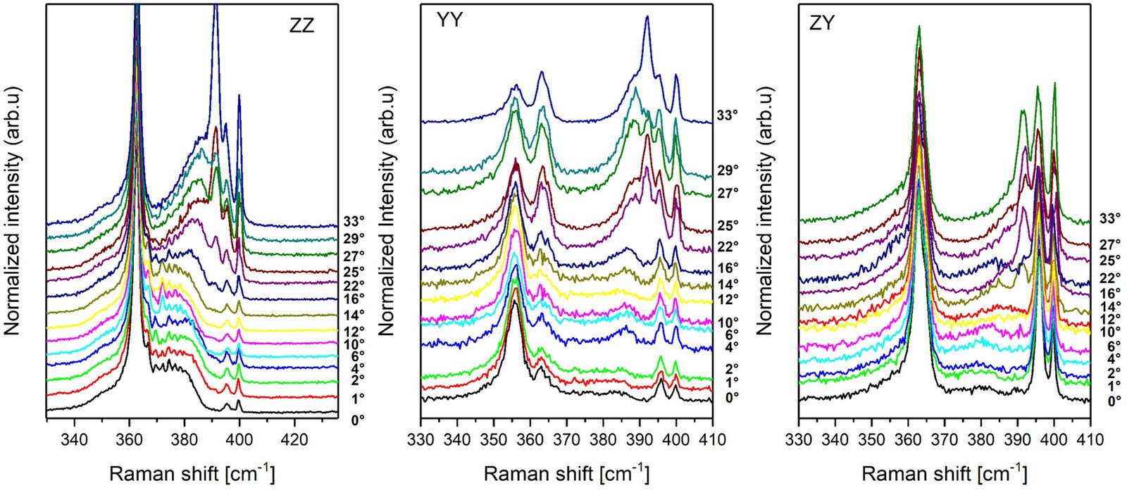
Upon varying the angle between the incident light and the nanowire growth axis, a systematic shift in the
polariton
mode
position is observed. This angular dependence modulates the resonance conditions, leading to the progressive
suppression
of surface phonon features in the Raman spectrum. Notably, as the polaritons mode approaches its convergence
limit, the
intensity of the LO phonon mode increases, and a resonant peak emerges—exceeding the intensity of both the LO
and TO modes.
Theoretically, as the convergence limit is approached, the two modes are expected to merge into a single
polaritonic
mode. However, this limit cannot be reached under the experimental conditions presented here. Nevertheless, at a
higher
incidence angle of 45°, the F-K phonon and the polariton features in the spectrum begin to merge, forming a
broader, more unified peak.
Measurement of GaP wired in cantilevered under ZZ polarization and incident angle, Theoretical dispersion of
F-K and polariton mode
While the above measurement proves the existence of SPhP resonance from both theoretical and experimental point
of view. The effect of the surrounding envirement is shown through spectral map of a cantilivered nanowire.
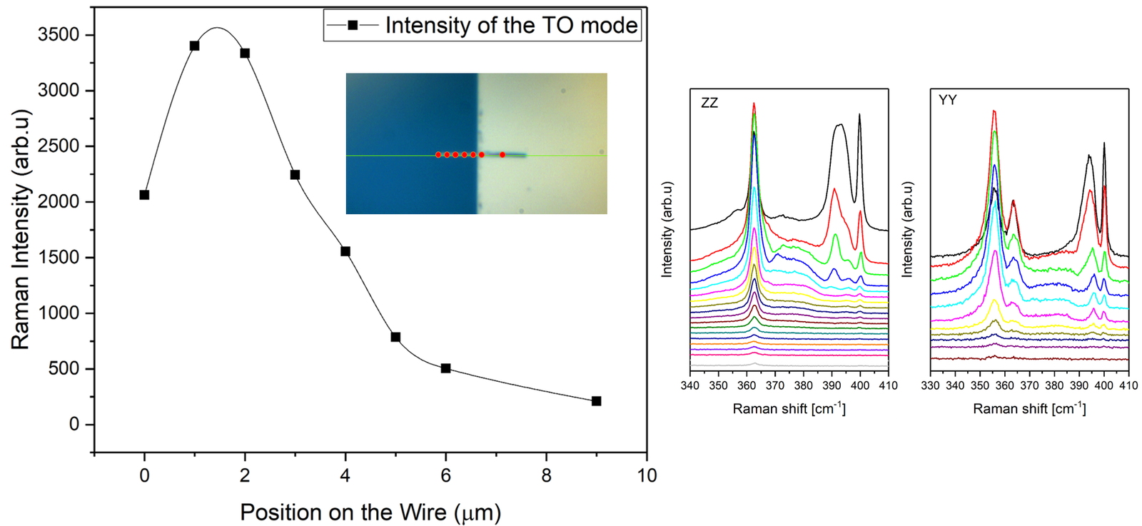
As the excitation spot approaches the substrate interface, a significant decrease (16-fold) in the overall Raman
signal is
observed, accompanied by the gradual disappearance of the surface phonon modes. This attenuation can be
attributed to
reduced light–matter interaction at the substrate boundary, increased optical losses, and possible disruption of
surface-specific vibrational coupling. This was observed on all the measured Nanowires under the cantilivered
configurations.
Mapping the GaP wired in cantilevered under ZZ and YY polarization
Variation of the TO intensity under ZZ polarization along the wire and the coresponding spectra in ZZ and YY
configuration
These measurements represents the first complete angular mapping of Raman spectral dependence, offering new
insights into
the anisotropic phonon behavior in nanostructures. It also opens promising avenues for future applications,
particularly
in the development of coherent thermal radiation sources to enhance heat dissipation at the nanoscale, and in
advancing
quantum sensing technologies through tailored phonon–photon interactions.
Let us know explore an other scenaria where a pure GaP wurzite Nanowire is placed on parallel strips of gold.
The reason behind this experiment is to investigate the role of alternating symmetric and asymetrical medium. As
shown above the SPhP should get surpressed when the Nanowire is in contact with a substate.
Raman map under ZZ polarization along the wire and the coresponding spectra in ZZ configuration in different
spots on the wire
A closer examination of the Raman intensity map reveals a clear periodicity in the surface phonon-polariton
(SPhP) mode.
Notably, the SPhP signal vanishes entirely when the nanowire is positioned on the gold strip, while a strong and
well-defined resonance is observed when the nanowire is suspended, clearly indicating the presence of a surface
phonon-polariton.
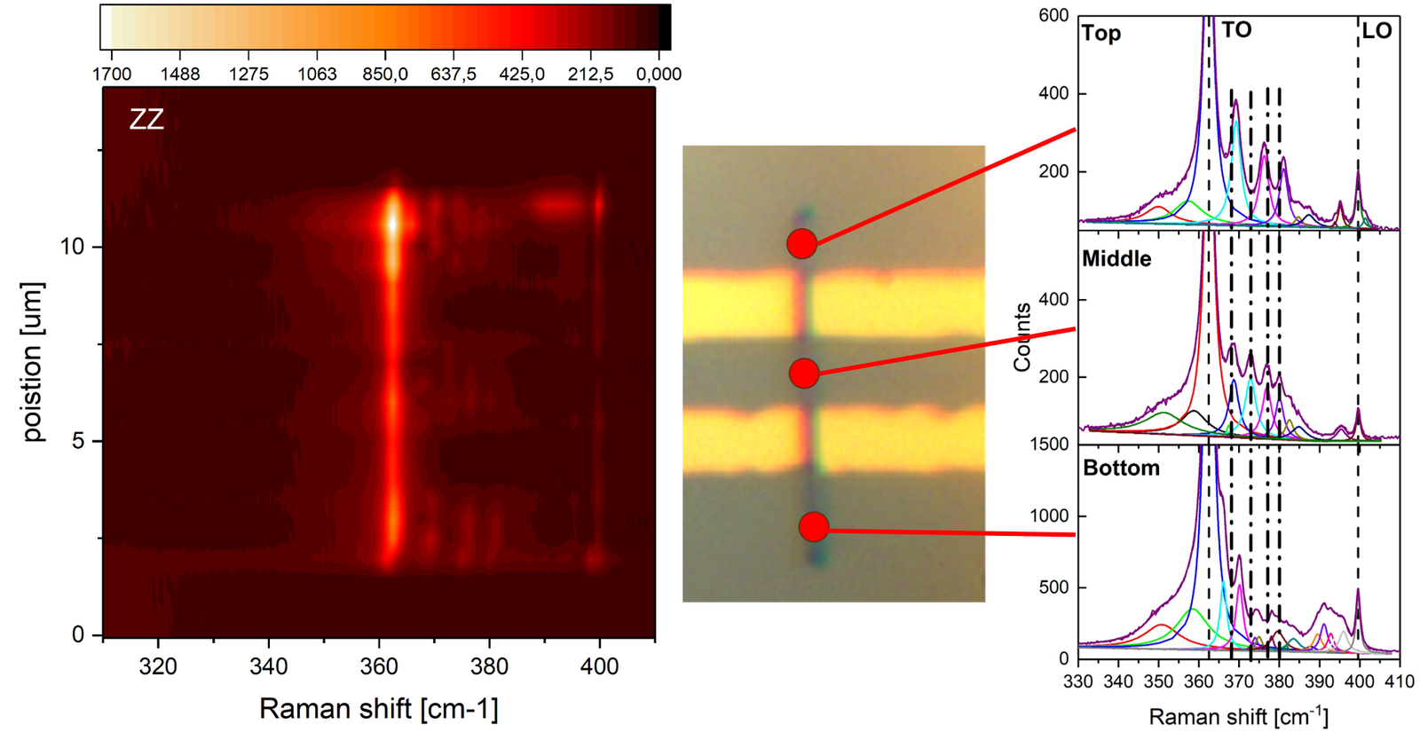
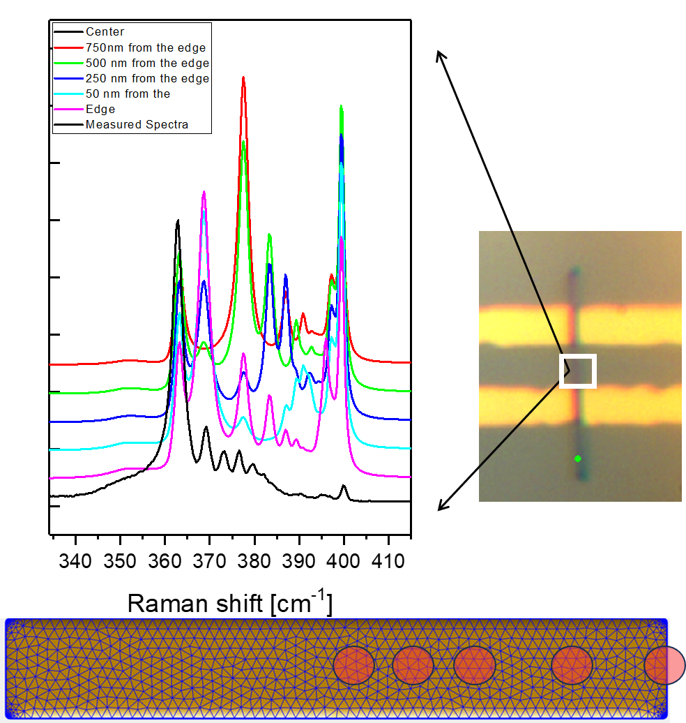
To better understand this behavior, a boundary element method (BEM) simulation was performed using
the
SPhP
Toolbox on a
GaP nano-rectangle. The simulation employed the refractive index values (n and k) characteristic of the wurtzite
phase,
which were extracted from fitting the experimental Raman spectra. The simulated structure had dimensions of 100 ×
150 ×
2000 nm. Spectra were calculated at several lateral positions: at the edge, and at 250 nm, 500 nm, 750 nm, and
at the
center of the nano-rectangle. Given the laser spot size (~920 nm), it is reasonable to assume that the measured
Raman
signal represents a spatial average, incorporating contributions from all these positions.
The results are shown below:
Raman map under ZZ polarization and the coresponding BEM simulation spectra collected along the rectangular
model
Conclusion
This work presents the first comprehensive angular mapping of surface phonon polaritons in GaP nanowires,
supported by
both theoretical modeling and experimental validation. It conclusively demonstrates that SPhPs are highly
sensitive to
dielectric environments, polarization, and incident angle, and can be selectively excited in suspended
geometries. The
findings highlight the potential of SPhPs for next-generation applications in coherent thermal radiation
control,
nanoscale heat dissipation, and quantum sensing, where controlled phonon–photon coupling is critical. These
insights
pave the way for engineering phononic and photonic devices that exploit surface vibrational modes at the
nanoscale.
← Back to Portfolio